TSMC Racing to 1nm, Investing $32 Billion for Fab: Report

(Image credit: TSMC)

In an interview, a vice prime minister of Taiwan said that TSMC had already made a strategic decision about where to build its fab capable of producing chips using 1nm-class (10 angstroms) fabrication technology in the second half of this decade. Still, these chip production facilities will be costly.

TSMC fabs that will make chips using its 1nm-class production nodes will be located near Longtan Science Park near Taoyuan, said Shen Jong-chin, vice prime minister of Taiwan, in an interview with Economic Daily (via Dan Nystedt). Of course, TSMC's plans have to be made official, and a lot may change by the time the world's largest foundry commits to the plan, but it looks like the company has already disclosed its general intentions to Taiwanese politicians.

Two major semiconductor production projects will create thousands of well-paid jobs, but they will also require investments previously not seen by the industry.

The vice prime minister estimates that TSMC must invest around $32 billion in a 1nm-capable fab. That's up from around $20 billion for N5 and N3 (5nm and 3nm-class) fabs that the company currently operates.

So far, TSMC has outlined plans to start making chips using its N2 (2nm-class) fabrication technology in the second half of 2025, which means that the first ICs made in the process will likely emerge on the market in 2026. N2 will be another long node for TSMC, and the company will offer multiple versions of the node, including those with gate-all-around transistors and backside power delivery.

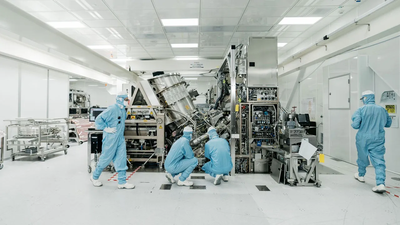
TSMC's N1 will follow N2 several years down the road. We do not know TSMC's exact plans concerning N1, but we think this fabrication process will be used to make ICs in 2027 ~ 2028. By the time ASML rolls out its extreme ultraviolet (EUV) lithography tools with High-NA. These will be costly scanners, making N1-capable fab very expensive too.

As a result, making chips at 10A process technology will be pricey, so do not expect many companies to adopt it due to prohibitively design and product costs.

In general, the vice PM believes that companies like TSMC, ASML, and Micron will have invested some $102.5 billion in the Taiwanese semiconductor industry, securing the country as the world's center of advanced semiconductor manufacturing.

Anton Shilov
Freelance News Writer

Anton Shilov is a Freelance News Writer at Tom’s Hardware US. Over the past couple of decades, he has covered everything from CPUs and GPUs to supercomputers and from modern process technologies and latest fab tools to high-tech industry trends.

  • peachpuff
    Intel: Behold... 10nm!
    Tsmc: :ROFLMAO:
    Reply
  • Co BIY
    Each doubling down on these process nodes is very risky. Someone (TSMC, Samsung or Intel) is likely to run into a limit either physical or financial where smaller isn't better.

    Much better to run the risk with government money !

    Of course then you have some government official blabbing your plans ahead of schedule.
    Reply
  • Bazzy 505
    amusingly enough even N5 TSMC is quite a misnomer, yes the single "fin" part is actually 5nm wide, but the minimum pitch between fins is 28nm, which translates average CGP of 51nm with cell height of 210nm . So there's really no such thing and 5nm transistor.
    But that doesn't translate into catchy marketing slongans that well.

    TSMC N5 is certainly a great achievement, but actual max logic density is around 137,6 MTr/mm2
    Intel 10mn SuperFin process node achieves max logic density 100.8 MTr/mm2 (rouhgly in ballpark of TSMC N7 process)

    so yeah it's one generation behind atm, but certainly not as far some would make you believe.

    Same story with so called 1nm is basically equivalent of 2 large molecules ;) till we know what real cell height is and actual min fin pitch, it's all just hot air ;)
    Reply
  • bit_user
    Co BIY said:
    Of course then you have some government official blabbing your plans ahead of schedule.
    A foundry needs to be fairly public about its plans, because it has to win new business from customers, and they tend to plan out their chip designs well in advance.

    Rest assured that all of the details TSMC discloses in its roadmaps are probably protected by several patents, each. And still, they don't reveal enough detail that someone else would easily be able to replicate the innovation.
    Reply
  • Marc9751
    Bazzy 505 said:
    amusingly enough even N5 TSMC is quite a misnomer, yes the single "fin" part is actually 5nm wide, but the minimum pitch between fins is 28nm, which translates average CGP of 51nm with cell height of 210nm . So there's really no such thing and 5nm transistor.
    But that doesn't translate into catchy marketing slongans that well.

    TSMC N5 is certainly a great achievement, but actual max logic density is around 137,6 MTr/mm2
    Intel 10mn SuperFin process node achieves max logic density 100.8 MTr/mm2 (rouhgly in ballpark of TSMC N7 process)

    so yeah it's one generation behind atm, but certainly not as far some would make you believe.

    Same story with so called 1nm is basically equivalent of 2 large molecules ;) till we know what real cell height is and actual min fin pitch, it's all just hot air ;)

    N5 is TSMC's latest node in 2019. However they've got 2 major node updates since then, N4(2021) and N3(2022).

    The timeline:
    2021 - Intel 7 (100.8 MTr/mm2)
    2021 - TSMC N4 (196.6 MTr/mm2)
    2022 - TSMC N3 (314.7 MTr/mm2) - entered volume production2023 - Intel 4 (160 MTr/mm2) - expected

    Even if Intel 4 successfully enter volume production in 2023, the density is still behind TSMC N4 node. I would say Intel is 2 nodes behind.
    Reply
  • Bazzy 505
    Marc9751 said:
    N5 is TSMC's latest node in 2019. However they've got 2 major node updates since then, N4(2021) and N3(2022).

    The timeline:
    2021 - Intel 7 (100.8 MTr/mm2)
    2021 - TSMC N4 (196.6 MTr/mm2) 146MTr/mm2 ( both N4 and N4P) (volume production in latter half 2022)2022 - TSMC N3 (314.7 MTr/mm2) - 220MTr/mm2 ( expected to enter volume production 2023)2023 - Intel 4 (160 MTr/mm2) - (expected to enter volume production in 2023)


    Even if Intel 4 successfully enter volume production in 2023, the density is still behind TSMC N4 node. I would say Intel is 2 nodes behind.

    N4 is still just a refinement of N5 5nm node (even tmsc itself lists it as such in their roadmaps) and you've got a transistor densities completely wrong for both N4 and N3
    so still 1 process node behind
    Reply