As desktop processors were first crossing the Gigahertz level, it seemed for a while that there was nowhere to go but up. But clock speed progress eventually ground to a halt, not because of anything to do with the speed itself but rather because of the power requirements and the heat all that power generated. Even with the now-common fans and massive heatsinks, along with some sporadic water cooling, heat remains a limiting factor that often throttles current processors.
Part of the problem with liquid cooling solutions is that they're limited by having to get the heat out of the chip and into the water in the first place. That has led some researchers to consider running the liquid through the chip itself. Now, some researchers from Switzerland have designed the chip and cooling system as a single unit, with on-chip liquid channels placed next to the hottest parts of the chip. The results are an impressive boost in heat-limited performance.
Feeling the heat
Part of our issue with getting heat out of a chip is that it usually involves multiple connections: from the chip to the chip packaging and the chip packaging to a heat sink. While steps can be made to improve these connections, there's an inefficiency to them, which adds up to limit the heat we can extract from the chip. This is true for the liquid cooling systems in current use, which use the liquid to replace the metal heat sink. While it might be possible to place the chip directly into a heat-conductive liquid, that liquid has to be an insulator and not undergo any chemical reactions with electronics components—both hurdles that water fails to clear.
There have been a number of demonstrations of on-chip liquid cooling. These typically involve a system where a device with a set of liquid channels is fused onto a chip, and a system pumps fluid through it. This can get heat off the chip, and initial implementations have found that there's a bit of a trade-off: it takes more power to pump the water through these channels than you extract from the processor. That power isn't used at the site where heat is an issue, so it doesn't get in the way of the heat dissipation, but it does cut into the energy efficiency of the system.
The new research builds upon these ideas to boost the efficiency of on-chip cooling systems. And the researchers involved demonstrate that it works using a power-converting chip that otherwise would see the performance reduced by the heat.
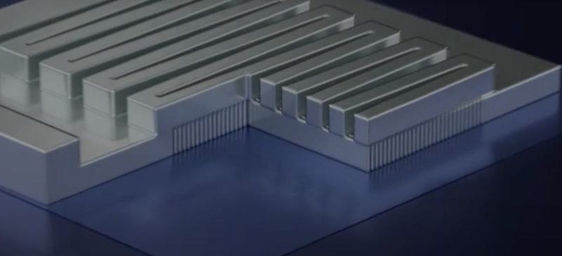
Etching a cooling system
Semiconductors used for power conversion tasks are typically not silicon. Instead, gallium nitride (GaN) is generally the choice, since it handles current better and reaches high frequencies. To maintain compatibility with existing fabrication approaches, however, most GaN devices are built on top of a silicon wafer, which simply provides physical support rather than contributing to the circuitry. To the researchers, the silicon provided an opportunity: we know how to control its structure at an extremely fine scale, which could be used to place coolant channels right up against the surface of the GaN circuitry.
The construction process is rather elaborate. Initially, extremely thin slits are cut through the GaN and into the underlying silicon. Then, an etching process that only affects silicon is used to widen these into channels, with the original gaps through the GaN layer sealed off with copper, which enhances the heat conduction into the water. Beneath these channels is a set of alternating passages that act as feeds and sinks. Cold water comes in via a feed, circulates up through the channel where it picks up heat, and then is drawn out through a neighboring sink.
The researchers arrange things so that the hottest parts of the GaN portion of the device are placed in close proximity to one of the channels, allowing a more efficient extraction of heat. A lot of the papers involve testing out different geometries of elements like the channel width and spacing. Throughout, the researchers tested the amount of energy required to force water through the system, which also put another constraint on the geometry. The best design they found is able to handle heat fluxes up to 1,700 watts per square centimeter while limiting the temperature rise of the chip to 60°C.
To turn this research into a useable device, the team used a thick double-sided adhesive layer and cut channels into that with a laser; the chip was then stuck down onto this adhesive. Water was pumped into the adhesive, from which it would flow into the chip. All of this was packaged onto a standard electronic board, with both leads for connecting it to power sources and valves that were used to feed the system water.
With the system in operation, temperature would rise by only about a third of a degree Celsius for each Watt of power it was handling. With a heat tolerance increase of 60°C, this meant the device could extract 176 watts while requiring a water flow of less than a milliliter per second. In addition, by keeping the heat limited, the circuitry performed its power conversion more efficiently.
Next steps
How big could this be? The authors cite estimates that about 30 percent of the energy use of data centers goes into cooling, and they use about 100 billion liters of water annually. If this technology could be adopted across all chips—not just power converters—it could drop the energy needed for cooling down to less than a percent of its current values.
But we're a long way off from that. For one thing, the researchers chose something that's extremely simple to test their system with, and that helped them design a cooling system that aligned with where the chip's hotspots were. Anything more complicated than that, and arranging the alignment could be considerably more difficult. This is especially true for general-purpose processors, where the parts of the chip being exercised may change based on workloads. The system will also need to be tested for its long-term stability, ensuring that its presence doesn't cause structural defects and that the interaction of high-temperature water with copper, silicon, and GaN doesn't lead to unforeseen problems.
Finally, there's the potential need to integrate sources and sinks for the water, perhaps multiple ones (power supply, GPU, processor), all at the appropriate pressures. So we're a long way off from seeing this turn up in any hardware. But it's at least nice to see a demonstration that the process can be done efficiently.
Nature, 2020. DOI: 10.1038/s41586-020-2666-1 (About DOIs).
reader comments
154